HIMNL9
0
- Joined
- May 26, 2009
- Messages
- 5,318
- Points
- 0
Ok, here's a "mini-review" (or, at least, the first part of it  ) of the pocket scope from JYETECH, the DIY kit version, including some pics (at the best that my webcam let me take them
  ) ..... and including, in the second part, some personal "hacking" of it, too (i always can't resist to try to "improve" something so cute, when i have it in my claws )
BTW, i'm not english, so, any grammatical error is a gift, ok ?
It come with the front and back panels, and a mini clip-type probe (also this DIY) ..... all the SMD components was taped on a paper foil, with their values and part numbers clearly indicated, so no confusions, at least if you proceed with a bit of order in soldering operations ..... dimensions of the scope are 65mm high x 107mm large (excluded the connectors), and the original depth was planned to be 28mm (but this don't take count of my hack, heheh).
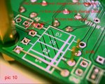
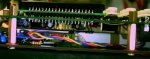
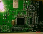
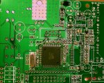
PCB is clean and well done (pic 1), only complain can be done for the lack of some indications in the serigraphic draws of the components ..... mean, there is the space for indicate better at least the polarity and part numbers of the biggest components ..... and the position of the calibration output (500 Hz 5 VPP), that is too near the switch ..... imho, it can be pulled until the switch side, between the first two switches, where there is a lot of space and nothing that interfer, but this is a choice of the maker, anyway ..... for the rest, the spaces between the components, also the SMD ones, looks enough for permit a clean assembly, and for not cause too much troubles in the soldering operations.
Also the SMD components are small, but "human size" ..... 1 x 2 mm can at least be handled, with a minimum of care, and luckily no components like the last 1 x 0.4mm ones, that are impossible to assemble correctly, hand way") ..... only the 3 switches looks a bit "weak", at first sight, but considering that, in the use, are protected from the front panel, they are robust enough, after all (just don't "cook" them heating them too much in the soldering operations, and all go fine).
..... only the 3 switches looks a bit "weak", at first sight, but considering that, in the use, are protected from the front panel, they are robust enough, after all (just don't "cook" them heating them too much in the soldering operations, and all go fine).
Another complain can be done about the front panel aperture for pass through the LCD ..... that don't pass through ..... mine is 1 mm more large of the LCD module, but is 0,5 mm less in height, so i had to file it away til the module is passed through ..... doing this handy, it's not the better aesthetic result, but there was no other way, if i want to keep the front panel (wondering if this is due to a different module in the previous versions, or just a mistake from the company that made the panels) ..... anyway, it's a venial sin, after all .
First operation to do, is check if there's ALL the parts that you need, inside the kit, checking both the parts list and the schematic ..... about this, i found that there was some lacking parts in the given SMD parts, compared with the schematic and the part / position lists, and being precise, c26 - c27 - c28 - dn2 - r19 - r26 - c19 - c6 - c2 - c4 (that are tracked on the PCB, but not included in the parts given), and r31, r70, jp2 (that are only in the schematic, but not more in the PCB tracks nor in the parts) ..... anyway, in the instructions there's specified to mount only the given parts, so probably the lacking ones are related to some modifications due to changes in firmware and/or revision, and not due to packing errors.
EDIT: For be sure, anyway, i asked to jyetech about that, and mr. Liu replied me (i got the reply right now) that those components was took out on purpose, and that must not be mounted, so it's all OK.
Also the wire modification reported in the instructions, is no more needed, cause it was needed only for old firmware releases.
Time to brick and mortar work (LOL j/k) ..... ok, for the assembly, you need a good quality soldering iron (that mean, thin tip ones, also 0,5mm or similar, are good for that work, if possible, temperature regulated), a sharp points tweezer, good quality multicore 0.5mm tin alloy wire (and i mean GOOD QUALITY, ok ?), and ofcourse, steady hands") ..... a suggestion, if you start to have some sight problems, or just want to see well what you're doing, get a +3 (3 dioptry) glasses from your optic store (those ready-to-go cheap glasses that are usually sold as spare glasses for few money), and use them as magnifiers ..... no, i'm not joking, they're very effective, and cheaper than a microscope or a professional magnifier headset (i NOT suggest you to use one of those magnifying glass plastic headsets, anyway, they're not really working good).
..... a suggestion, if you start to have some sight problems, or just want to see well what you're doing, get a +3 (3 dioptry) glasses from your optic store (those ready-to-go cheap glasses that are usually sold as spare glasses for few money), and use them as magnifiers ..... no, i'm not joking, they're very effective, and cheaper than a microscope or a professional magnifier headset (i NOT suggest you to use one of those magnifying glass plastic headsets, anyway, they're not really working good).
Some suggestions that i use for SMD mounting without machines (handy made), those anyway are personal things, and anyone have their systems, so take mine as just as sugestions ..... also, i'm pretty sure that most of you already know all those things, but, please, don't feel my suggestions offensive just cause they say things that you already know ..... cause there's always someone that may not know some of these things, and a suggestion that is already known from 99 peoples, can always be helpful for the remaining one, ok ?
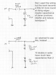
Better start pre-tinning ONE of the soldering pads of each components, and TWO (diagonally opposite) or ALL of the soldering pads of integrated circuits (this depend from what system you use for solder them, i personally prefer tin all), putting very few tin on the interested pads ..... this permit you to fix in place the component, before finally solder it, aligning them good enough for avoid accidental short-circuits (like in the attacked images) ..... if you put too much tin on a pad or make shorts, don't use desoldering tools, just revert the PCB, and take it away with the soldering iron (the gravity is your friend, here ..... look the draw 1, and sorry, but i'm not too good drawing freehand), this left on the pad just the amount of tin that you need, usually (look at pic 2, you can see indicatively how much tin you need) ..... also, remember to never press too much on the pads, nor "scratch" them with the soldering iron, tinning them, nor keep the soldering iron too much time on the pads overheating and "cooking" them, cause this can provoke the detachments of the copper layer from the vetronite (fiberglass) support board, and if this happen in critic places, you waste all your work and may have to throw away your kit.
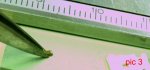
Start with the resistors (just cause they're the more low components ..... ALWAYS try to start from low components, so the mounted ones don't interfer with the mount of the next ones), and start from the top of the list, one value at time, mounting all the similar values all together (and NOT following the progressive part numbers), before detach and open the next value, so you can't make confusion with different values ..... also, a little piece of silicone pad, or any other anti-skid pad, is very helpful managing the SMD parts handy, due to their small sizes and lightweight ..... when you open one of the small cardboard holder of the components, just left all the components go on the pad, so they don't go here and there and you can manage them with pliers ..... like pic 3, as example, that was C3 ..... don't know in your country, but as example, here there was sold here and there things called "anti skid pad for gps receivers", that was used for keep the bluetooth gps receivers fixed, when used in cars, and not let them slip here and there when you drive in curves ..... those pads are perfects also for manage SMD components in that way, but any silicone pads can work good enough
Just take your components as in figure, align them with the pads (in their right place, ofcourse), and solder the side where you had tinned the pad, keeping the component as more flat possible ..... then, pressing gently on the component with the tweezers, heat again briefly the pad, so the component go down flat on the PCB, then solder the opposite side, and finally, if you want, put another little amount of tin on the first side (just in case the tin was not enough) ..... solder your components one by one, being sure to have soldered both the sides, before pass to another ..... don't be tempted to just put all the ones on the pcb soldering just one side, saying that you can have time to solder the other side all together, cause it's really too easy, with SMD components, just forgot one for distraction
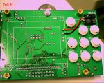
Once you've soldered all the resistors (pic 2 shows the PCB with only the resistors on it), pass to the capacitors, always following the part order, the inductances, then the semiconductors (pic 4), and for the last ones, the 3 integrated circuits (pic 5) ..... as you can see, it's not so difficult.
For solder the integrated circuits, i personally prefer this system (having pre-tinned all the pads, ofcourse): align the IC with the pins perfectly aligned on the soldering pads of the PCB (and, ofcourse, IN THE RIGHT SENSE, cause once you've soldered them, it's too late for notice that you've soldered it reversed), keep it pressed on the pcb firmly with a finger, then solder the pin in one corner, then rotate the PCB, press it down again (always keep the alignment !), and solder the pin in the opposite diagonal corner ..... this keep the IC aligned for the operation on the other pins ..... at this point, keeping it pushed down on the PCB, just solder the remaining pins one by one .
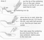
A good way for solder those types of pins is starting heating the pad where it's not covered from the pin with the tip of the solderin iron, then when the tin melt, move the soldering iron tip against the pin, wait half second or similar, til the pin heat enough and become soldered, and when it's soldered, take away the tip, wait 2 or 3 seconds for left it cool a bit, then do the same with the subsequent pin, and so on ..... this do a good operation and at the same time prevent you to overheat the IC, and it's a good way for avoid to make "bridges" of tin between two pins, thing that is more easy to do adding the tin as in normal soldering procedures (look also the draw 2, it's more clear) ..... only, don't push too hard with the tip on the pads ..... touching firmly, but not scratching them, it's the secret ..... i use this system from a lot of time, and til now, never failed
A pair of notes, about diodes ..... they indicate the anode of the diodes, as opposite of the international convention that always indicate the cathode, so pay attention to the circuit ..... D7 go with the anode, where on the PCB is drawed the symbol of the rounded corners of it, instead the cathode (mean, the side with the cathode strip mark, go in the direction of Q1, not in the direction of C14 and L2) ..... same, for the D1, the anode is in the direction of C12, and the strip that mark the cathode is in direction of R12 ..... don't invert them, or the scope don't work ..... and just in case you're searching L2, it's not SMD, it's a normal component, without any value printed on it, mixed with all the rest in the plastic bag ..... another thing, that is indexed also in the instructions, is that you have to mount C14 reversed ..... usually the convention is that the positive pin of the polarized capacitors must be mounted in the square pad, that index the +, but for an error, the pads of C14 was exchanged, so mount it with the negative pin in the square pad.
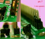
Once you've mounted all the SMD parts, pass to mount L2, the electrolitic capacitors, that go mounted with positive pin on the square pads, EXCEPT C14, as said, and the led (also for this, the dot on the PCB indicate the anode, instead that the cathode, anyway the cathode go in direction of C11), and the 10 pins connector, that is needed if you have to reprogram the Altera processor or change firmware version ..... after the soldering operations, cut the pins exceeding from the other side, using a GOOD snipper, around 1 mm from the PCB, also 0,5mm, if you can do that, but not more short, if you're not used to work in this way ..... anyway, you need to cut them, cause some of them remains under the LCD panel, and you must not risk to short something under it with a too long remained pin.
The diodes 1N4001, need to decide how you want to power the scope, for decide what mount or not mount ..... if you plan to use an AC power supply, mount all them (but if you're using AC, i suggest you to not go over 7,5 Volt), if you want to power it using a DC power supply, just mount D3, and short circuit D4 with a piece of wire (or the cutted terminal of a component) and use a stabilized 9 Volts DC power supply, that is the better choice.
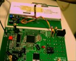
Note that my pics looks a bit differents, but that it's due to the fact that i need to mount it in an inusual way, for my hacking idea ..... that what i'm describing here, actually, it's the normal way for mount it, for those that are not crazy like me ..... after, when i have time to finish all, i describe also the hacked part, but need some time for complete all .
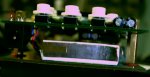
Now you can revert the PCB and solder the other parts, switches and pushbuttons ..... pushbuttons, as you can note trying to insert them, have the pins that are half millimeter more large than the holes in pcb, but is enough insert them carefully and gently push them til they are flat on the pcb, and them remains in place, so solder them is not a problem ..... only, never try to bend their terminals, cause they are crude phosphorous bronze, not copper, and bending them, you risk to break them away from the button, also bending them only one time ..... switches instead need to be kept aligned and pushed down at least til you've soldered one or two pins, for a good result (and remember that all them must be soldered on the opposite side, not where you've soldered the components) ..... cause there's a lot of space, there, you can snip the pins also from them, or just left them untouched, it's not important.
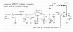
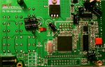
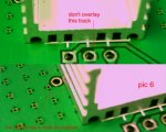
7805 voltage regulator require a pair of words, too ..... as you can see, there's space for mount it barely on the PCB, or for mount it with a little heatsink, that is better if you use more than 9 Volt as power supply ..... as you can see in pic 6, if you use the heatsink, you must keep it aligned with the external border of the PCB, so the inside part don't overlay the track from the IN pin of the regulator ..... this, cause also if there is solder on the PCB, it can always be scratched away, and if this happen and the heatsink go short circuit the track, your scope can smoke, but difficult can work ..... also, mounting the heatsink, you have to cut away one of the pins from the LCD module, otherwise you can't align it completely, cause the heatsink cover the related hole.
And for the regulator itself, don't just bend the pins raw against the body, otherwise you risk to break them away, and anyway they remain too near the heatsink ..... just use a thin plier, or a spacer, and bend them lefting 1 to 1,5mm from the pins and the body.
Time to wash all ..... seriously, solder paste residuals can alter the work of the circuits, especially at high frequencies, so, if you want a better result, wash away all the solder desoxidant residuals ..... if you don't have freon or other specific products, a good alternative is using a dry contact cleaner, like philips R21 or similars, that can melt the desoxidant paste without ruin the other electronic parts, and a brush ..... put the PCB flat, spray the cleaner on it (be also abundant), and brush all with the brush, til all the residuals melts ..... keep it wet with cleaner, cause it evaporate very quick, and at last, lift the PCB from a corner and spray again all the components, til it's clean (must not remain "sticky" tracks, preferably), and blow it with air, if you want, at the end.
Til now, it's all, need some time for assemble the rest, but have also to run a pc shop all alone, so can't do all that what i want all together, sorry ..... next step tomorrow, promised
) of the pocket scope from JYETECH, the DIY kit version, including some pics (at the best that my webcam let me take them ) ..... and including, in the second part, some personal "hacking" of it, too (i always can't resist to try to "improve" something so cute, when i have it in my claws )BTW, i'm not english, so, any grammatical error is a gift, ok ?
It come with the front and back panels, and a mini clip-type probe (also this DIY) ..... all the SMD components was taped on a paper foil, with their values and part numbers clearly indicated, so no confusions, at least if you proceed with a bit of order in soldering operations ..... dimensions of the scope are 65mm high x 107mm large (excluded the connectors), and the original depth was planned to be 28mm (but this don't take count of my hack, heheh).
PCB is clean and well done (pic 1), only complain can be done for the lack of some indications in the serigraphic draws of the components ..... mean, there is the space for indicate better at least the polarity and part numbers of the biggest components ..... and the position of the calibration output (500 Hz 5 VPP), that is too near the switch ..... imho, it can be pulled until the switch side, between the first two switches, where there is a lot of space and nothing that interfer, but this is a choice of the maker, anyway ..... for the rest, the spaces between the components, also the SMD ones, looks enough for permit a clean assembly, and for not cause too much troubles in the soldering operations.
Also the SMD components are small, but "human size" ..... 1 x 2 mm can at least be handled, with a minimum of care, and luckily no components like the last 1 x 0.4mm ones, that are impossible to assemble correctly, hand way
..... only the 3 switches looks a bit "weak", at first sight, but considering that, in the use, are protected from the front panel, they are robust enough, after all (just don't "cook" them heating them too much in the soldering operations, and all go fine).Another complain can be done about the front panel aperture for pass through the LCD ..... that don't pass through
..... mine is 1 mm more large of the LCD module, but is 0,5 mm less in height, so i had to file it away til the module is passed through ..... doing this handy, it's not the better aesthetic result, but there was no other way, if i want to keep the front panel (wondering if this is due to a different module in the previous versions, or just a mistake from the company that made the panels) ..... anyway, it's a venial sin, after all .First operation to do, is check if there's ALL the parts that you need, inside the kit, checking both the parts list and the schematic ..... about this, i found that there was some lacking parts in the given SMD parts, compared with the schematic and the part / position lists, and being precise, c26 - c27 - c28 - dn2 - r19 - r26 - c19 - c6 - c2 - c4 (that are tracked on the PCB, but not included in the parts given), and r31, r70, jp2 (that are only in the schematic, but not more in the PCB tracks nor in the parts) ..... anyway, in the instructions there's specified to mount only the given parts, so probably the lacking ones are related to some modifications due to changes in firmware and/or revision, and not due to packing errors.
EDIT: For be sure, anyway, i asked to jyetech about that, and mr. Liu replied me (i got the reply right now) that those components was took out on purpose, and that must not be mounted, so it's all OK.
Also the wire modification reported in the instructions, is no more needed, cause it was needed only for old firmware releases.
Time to brick and mortar work (LOL j/k) ..... ok, for the assembly, you need a good quality soldering iron (that mean, thin tip ones, also 0,5mm or similar, are good for that work, if possible, temperature regulated), a sharp points tweezer, good quality multicore 0.5mm tin alloy wire (and i mean GOOD QUALITY, ok ?), and ofcourse, steady hands
..... a suggestion, if you start to have some sight problems, or just want to see well what you're doing, get a +3 (3 dioptry) glasses from your optic store (those ready-to-go cheap glasses that are usually sold as spare glasses for few money), and use them as magnifiers ..... no, i'm not joking, they're very effective, and cheaper than a microscope or a professional magnifier headset (i NOT suggest you to use one of those magnifying glass plastic headsets, anyway, they're not really working good).Some suggestions that i use for SMD mounting without machines (handy made
), those anyway are personal things, and anyone have their systems, so take mine as just as sugestions ..... also, i'm pretty sure that most of you already know all those things, but, please, don't feel my suggestions offensive just cause they say things that you already know ..... cause there's always someone that may not know some of these things, and a suggestion that is already known from 99 peoples, can always be helpful for the remaining one, ok ? Better start pre-tinning ONE of the soldering pads of each components, and TWO (diagonally opposite) or ALL of the soldering pads of integrated circuits (this depend from what system you use for solder them, i personally prefer tin all), putting very few tin on the interested pads ..... this permit you to fix in place the component, before finally solder it, aligning them good enough for avoid accidental short-circuits (like in the attacked images) ..... if you put too much tin on a pad or make shorts, don't use desoldering tools, just revert the PCB, and take it away with the soldering iron (the gravity is your friend, here ..... look the draw 1, and sorry, but i'm not too good drawing freehand), this left on the pad just the amount of tin that you need, usually (look at pic 2, you can see indicatively how much tin you need) ..... also, remember to never press too much on the pads, nor "scratch" them with the soldering iron, tinning them, nor keep the soldering iron too much time on the pads overheating and "cooking" them, cause this can provoke the detachments of the copper layer from the vetronite (fiberglass) support board, and if this happen in critic places, you waste all your work and may have to throw away your kit.
Start with the resistors (just cause they're the more low components ..... ALWAYS try to start from low components, so the mounted ones don't interfer with the mount of the next ones), and start from the top of the list, one value at time, mounting all the similar values all together (and NOT following the progressive part numbers), before detach and open the next value, so you can't make confusion with different values ..... also, a little piece of silicone pad, or any other anti-skid pad, is very helpful managing the SMD parts handy, due to their small sizes and lightweight ..... when you open one of the small cardboard holder of the components, just left all the components go on the pad, so they don't go here and there and you can manage them with pliers ..... like pic 3, as example, that was C3 ..... don't know in your country, but as example, here there was sold here and there things called "anti skid pad for gps receivers", that was used for keep the bluetooth gps receivers fixed, when used in cars, and not let them slip here and there when you drive in curves ..... those pads are perfects also for manage SMD components in that way, but any silicone pads can work good enough
Just take your components as in figure, align them with the pads (in their right place, ofcourse
), and solder the side where you had tinned the pad, keeping the component as more flat possible ..... then, pressing gently on the component with the tweezers, heat again briefly the pad, so the component go down flat on the PCB, then solder the opposite side, and finally, if you want, put another little amount of tin on the first side (just in case the tin was not enough) ..... solder your components one by one, being sure to have soldered both the sides, before pass to another ..... don't be tempted to just put all the ones on the pcb soldering just one side, saying that you can have time to solder the other side all together, cause it's really too easy, with SMD components, just forgot one for distraction Once you've soldered all the resistors (pic 2 shows the PCB with only the resistors on it), pass to the capacitors, always following the part order, the inductances, then the semiconductors (pic 4), and for the last ones, the 3 integrated circuits (pic 5) ..... as you can see, it's not so difficult
.For solder the integrated circuits, i personally prefer this system (having pre-tinned all the pads, ofcourse): align the IC with the pins perfectly aligned on the soldering pads of the PCB (and, ofcourse, IN THE RIGHT SENSE, cause once you've soldered them, it's too late for notice that you've soldered it reversed
), keep it pressed on the pcb firmly with a finger, then solder the pin in one corner, then rotate the PCB, press it down again (always keep the alignment !), and solder the pin in the opposite diagonal corner ..... this keep the IC aligned for the operation on the other pins ..... at this point, keeping it pushed down on the PCB, just solder the remaining pins one by one .A good way for solder those types of pins is starting heating the pad where it's not covered from the pin with the tip of the solderin iron, then when the tin melt, move the soldering iron tip against the pin, wait half second or similar, til the pin heat enough and become soldered, and when it's soldered, take away the tip, wait 2 or 3 seconds for left it cool a bit, then do the same with the subsequent pin, and so on ..... this do a good operation and at the same time prevent you to overheat the IC, and it's a good way for avoid to make "bridges" of tin between two pins, thing that is more easy to do adding the tin as in normal soldering procedures (look also the draw 2, it's more clear) ..... only, don't push too hard with the tip on the pads ..... touching firmly, but not scratching them, it's the secret ..... i use this system from a lot of time, and til now, never failed
A pair of notes, about diodes ..... they indicate the anode of the diodes, as opposite of the international convention that always indicate the cathode, so pay attention to the circuit ..... D7 go with the anode, where on the PCB is drawed the symbol of the rounded corners of it, instead the cathode (mean, the side with the cathode strip mark, go in the direction of Q1, not in the direction of C14 and L2) ..... same, for the D1, the anode is in the direction of C12, and the strip that mark the cathode is in direction of R12 ..... don't invert them, or the scope don't work ..... and just in case you're searching L2, it's not SMD, it's a normal component, without any value printed on it, mixed with all the rest in the plastic bag
..... another thing, that is indexed also in the instructions, is that you have to mount C14 reversed ..... usually the convention is that the positive pin of the polarized capacitors must be mounted in the square pad, that index the +, but for an error, the pads of C14 was exchanged, so mount it with the negative pin in the square pad.Once you've mounted all the SMD parts, pass to mount L2, the electrolitic capacitors, that go mounted with positive pin on the square pads, EXCEPT C14, as said, and the led (also for this, the dot on the PCB indicate the anode, instead that the cathode, anyway the cathode go in direction of C11), and the 10 pins connector, that is needed if you have to reprogram the Altera processor or change firmware version ..... after the soldering operations, cut the pins exceeding from the other side, using a GOOD snipper, around 1 mm from the PCB, also 0,5mm, if you can do that, but not more short, if you're not used to work in this way ..... anyway, you need to cut them, cause some of them remains under the LCD panel, and you must not risk to short something under it with a too long remained pin.
The diodes 1N4001, need to decide how you want to power the scope, for decide what mount or not mount ..... if you plan to use an AC power supply, mount all them (but if you're using AC, i suggest you to not go over 7,5 Volt), if you want to power it using a DC power supply, just mount D3, and short circuit D4 with a piece of wire (or the cutted terminal of a component) and use a stabilized 9 Volts DC power supply, that is the better choice.
Note that my pics looks a bit differents, but that it's due to the fact that i need to mount it in an inusual way, for my hacking idea ..... that what i'm describing here, actually, it's the normal way for mount it, for those that are not crazy like me ..... after, when i have time to finish all, i describe also the hacked part, but need some time for complete all
.Now you can revert the PCB and solder the other parts, switches and pushbuttons ..... pushbuttons, as you can note trying to insert them, have the pins that are half millimeter more large than the holes in pcb, but is enough insert them carefully and gently push them til they are flat on the pcb, and them remains in place, so solder them is not a problem ..... only, never try to bend their terminals, cause they are crude phosphorous bronze, not copper, and bending them, you risk to break them away from the button, also bending them only one time ..... switches instead need to be kept aligned and pushed down at least til you've soldered one or two pins, for a good result (and remember that all them must be soldered on the opposite side, not where you've soldered the components
) ..... cause there's a lot of space, there, you can snip the pins also from them, or just left them untouched, it's not important.7805 voltage regulator require a pair of words, too ..... as you can see, there's space for mount it barely on the PCB, or for mount it with a little heatsink, that is better if you use more than 9 Volt as power supply ..... as you can see in pic 6, if you use the heatsink, you must keep it aligned with the external border of the PCB, so the inside part don't overlay the track from the IN pin of the regulator ..... this, cause also if there is solder on the PCB, it can always be scratched away, and if this happen and the heatsink go short circuit the track, your scope can smoke, but difficult can work
..... also, mounting the heatsink, you have to cut away one of the pins from the LCD module, otherwise you can't align it completely, cause the heatsink cover the related hole.And for the regulator itself, don't just bend the pins raw against the body, otherwise you risk to break them away, and anyway they remain too near the heatsink ..... just use a thin plier, or a spacer, and bend them lefting 1 to 1,5mm from the pins and the body.
Time to wash all ..... seriously, solder paste residuals can alter the work of the circuits, especially at high frequencies, so, if you want a better result, wash away all the solder desoxidant residuals ..... if you don't have freon or other specific products, a good alternative is using a dry contact cleaner, like philips R21 or similars, that can melt the desoxidant paste without ruin the other electronic parts, and a brush ..... put the PCB flat, spray the cleaner on it (be also abundant), and brush all with the brush, til all the residuals melts ..... keep it wet with cleaner, cause it evaporate very quick, and at last, lift the PCB from a corner and spray again all the components, til it's clean (must not remain "sticky" tracks, preferably), and blow it with air, if you want, at the end.
Til now, it's all, need some time for assemble the rest, but have also to run a pc shop all alone, so can't do all that what i want all together, sorry ..... next step tomorrow, promised
Attachments


Last edited: