Hello Guys,
as I learned very much from the knowledge thats stored in the forum, I want to give something back.
I made some experiments and can now say that I fully understand the so called box reflection.
I do also have a way to eliminate it. Its not easy however.
But first the basics.
I took a 445nm Laserdiode and decanned it. Its a 1,6W Osram.

Almost everybody has seen something like this before.
Also the Box reflection, hard to photograph. This picture is just below threshold, so actually not lasing.

The dreaded box that kills the clean beams we all like. Hated by many..
This is a picture of the diode actually lasing. Its a 488nm 55mW this time. But the box is the same on other diodes.

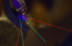
So what's actually happening? First we need to look at the source. I made some notes to explain the parts we can see and identify.

As you can see, the actual laser is just the box thats on top of the base substrate. A small bar shaped object with some electric contacts on top and on the bottom. A picture from the front will show the output of the laser die in its full glory.

This picture is a little misleading, the bright blue spot is not actually the output of the laserdiode. Its not running at full current right now, so the laser diode is not lasing, just led action here. The current is very low, just a few mA. This makes the active area not light up fully and evenly. Its lighting more in places where the current density is higher. Regions with defects will glow less. This makes it seem like the actual lasing output is not centered, but this is not the case.
EDIT: See below, thats actually not the case here, this diode is asymmetric, however it still does not light evenly, next picture shows a bright spot far right but no light inbetween. So the bright blue spot is actually the lasing output area.

You can also see the n-substrate glowing slightly here. Actually the whole front of the laser die is glowing slightly. The bottom N portion is actually transparent and therefor the cause of our box reflection. The next picture shows a shematical drawing. The blue striped block shows the n-substrate thats transparent and beneath the actual active area.
The active area is actually the whole stripe between the n and p (green). Its just not lasing everywhere, because the current density is not big enough in these areas.

If we overlay the box reflection picture its more clear.

As we can see, the collimating lens is just imaging the whole crystal / laser die. As the bottom n- substrate is also glowing, its projecting the image of this. The line thats left/right from the dot is also just the active area led-ing.
So what can we do about that?
Not much, but there is a way.
We could insert a piece of metal between the collimating lens and the die. It would need to be positioned as close to the die as possible, so decanning is necessary. It also would need to be positioned quite accurately, way to accurate for me.
However if done right, it should block all light from the n-substrate thus cleaning up the beam.
I tested this, I couldn't get the alignment right but I could prove the concept. To clean up the side lines, one would also need some form of beam block on the side of the die.
There is also a different form of reflection. The laser die actually also emits light on the back side. This can also be seen in the first picture. This light is also getting out of the collimating lens. However its very faint and not in focus because the light source is actually a few mm behind the focal plane. This light spreads very fast. I can only be seen if you have a very short distance between your diode and the projection screen. If you look closely, you can see the shadow of the bond wires. This light could be reduced by painting the back of the housing black. It works but is not necessary because its so faint.
I hope everybody understands there diodes just a little better after this.
Have a nice day
Farbe
as I learned very much from the knowledge thats stored in the forum, I want to give something back.
I made some experiments and can now say that I fully understand the so called box reflection.
I do also have a way to eliminate it. Its not easy however.
But first the basics.
I took a 445nm Laserdiode and decanned it. Its a 1,6W Osram.
Almost everybody has seen something like this before.
Also the Box reflection, hard to photograph. This picture is just below threshold, so actually not lasing.
The dreaded box that kills the clean beams we all like. Hated by many..
This is a picture of the diode actually lasing. Its a 488nm 55mW this time. But the box is the same on other diodes.
So what's actually happening? First we need to look at the source. I made some notes to explain the parts we can see and identify.
As you can see, the actual laser is just the box thats on top of the base substrate. A small bar shaped object with some electric contacts on top and on the bottom. A picture from the front will show the output of the laser die in its full glory.
This picture is a little misleading, the bright blue spot is not actually the output of the laserdiode. Its not running at full current right now, so the laser diode is not lasing, just led action here. The current is very low, just a few mA. This makes the active area not light up fully and evenly. Its lighting more in places where the current density is higher. Regions with defects will glow less. This makes it seem like the actual lasing output is not centered, but this is not the case.
EDIT: See below, thats actually not the case here, this diode is asymmetric, however it still does not light evenly, next picture shows a bright spot far right but no light inbetween. So the bright blue spot is actually the lasing output area.
You can also see the n-substrate glowing slightly here. Actually the whole front of the laser die is glowing slightly. The bottom N portion is actually transparent and therefor the cause of our box reflection. The next picture shows a shematical drawing. The blue striped block shows the n-substrate thats transparent and beneath the actual active area.
The active area is actually the whole stripe between the n and p (green). Its just not lasing everywhere, because the current density is not big enough in these areas.
If we overlay the box reflection picture its more clear.
As we can see, the collimating lens is just imaging the whole crystal / laser die. As the bottom n- substrate is also glowing, its projecting the image of this. The line thats left/right from the dot is also just the active area led-ing.
So what can we do about that?
Not much, but there is a way.
We could insert a piece of metal between the collimating lens and the die. It would need to be positioned as close to the die as possible, so decanning is necessary. It also would need to be positioned quite accurately, way to accurate for me.
However if done right, it should block all light from the n-substrate thus cleaning up the beam.
I tested this, I couldn't get the alignment right but I could prove the concept. To clean up the side lines, one would also need some form of beam block on the side of the die.
There is also a different form of reflection. The laser die actually also emits light on the back side. This can also be seen in the first picture. This light is also getting out of the collimating lens. However its very faint and not in focus because the light source is actually a few mm behind the focal plane. This light spreads very fast. I can only be seen if you have a very short distance between your diode and the projection screen. If you look closely, you can see the shadow of the bond wires. This light could be reduced by painting the back of the housing black. It works but is not necessary because its so faint.
I hope everybody understands there diodes just a little better after this.
Have a nice day
Farbe
Last edited: